

")

Frequently Asked Questions about IS200JPDEG1A
How does this IS200JPDEG1A board’s normal coating style compare to the alternative conformal style of PCB coating?
How does the IS200JPDEG1A process signal feedback?
How many inputs does the IS200JPDEG1A have for power supplies?
Hardware Tips and Specifications
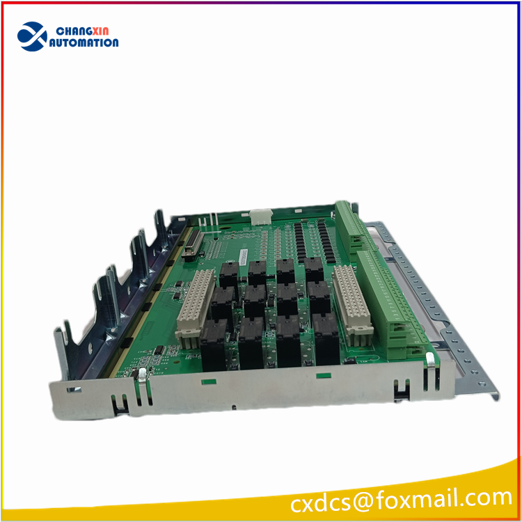
The IS200JPDEG1A board’s functional description as a DC Battery Power Distribution Board explains its functionality well; the IS200JPDEG1A PCB exists with the purpose of distributing DC power from a battery or power supply to various system loads, including most Mark VIe Series terminal board products.
This IS200JPDEG1A PCB makes use of two 50-pin diagnostic pin connectors which jut out at the top and bottom of the base circuit board. These connectors, labeled P1 and P2 respectively, each offer the IS200JPDEG1A board with feedback signal transmission and reception options, specifically geared towards the related PPDA Input/Output Pack.

There are no reviews yet.